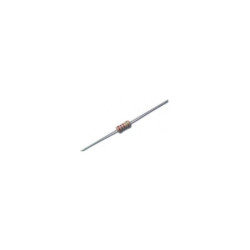
Flip Flop dual J-K con preset y clear. 74112. J-37
DUAL J-K FLIP FLOP WITH PRESET AND CLEAR
HIGH SPEED fMAX = 67 MHz (TYP.) AT VCC 5 V LOW POWER DISSIPATION ICC 25 °C HIGH NOISE IMMUNITY VNIH = VNIL 28 % VCC (MIN.) OUTPUT DRIVE CAPABILITY 10 LSTTL LOADS SYMMETRICAL OUTPUT IMPEDANCE |IOH| = IOL 4 mA (MIN.) BALANCED PROPAGATION DELAYS tPLH = tPHL WIDE OPERATING VOLTAGE RANGE VCC (OPR) 6 V PIN AND FUNCTION COMPATIBLE WITH 54/74LS112
DESCRIPTION The is a high speed CMOS DUAL J-K FLIP-FLOP WITH PRESET AND CLEAR fabricated in silicon gate C2MOS technology. It has the same high speed performance of LSTTL combined with true CMOS low power consumption. The M54HC112/M74HC112 dual JK flip-flop features individual J,K, clock, and asynchronous set and clearinputs for each flip-flop. When the clock goes high, the inputs are enabled and data will be accepted. The logic level of the J and K inputs may be allowed to change when the clock pulse is high and the bistable will function as shown in the truth table. Input data is transferred to the input on the negative going edge of the clock pulse. All inputs are equipped withprotection circuits against static discharge and transient excess voltage. INPUT AND OUTPUT EQUIVALENT CIRCUIT
PIN No SYMBOL 1CLR, 2CLR GND V CC NAME AND FUNCTION Clock Input (HIGH to LOW edge triggered) Data Inputs: Flip-Flop 1 and 2 Data Inputs: Flip-Flop 1 and 2 Set Inputs True Flip-Flop Outputs Complement Flip-Flop Outputs Reset inputs Ground (0V) Positive Supply Voltage
Symbol VCC VI VO IIK IOK IO ICC or IGND PD Tstg TL Supply Voltage DC Input Voltage DC Output Voltage DC Input Diode Current DC Output Diode Current DC Output Source Sink Current Per Output Pin DC VCC or Ground Current Power Dissipation Storage Temperature Lead Temperature (10 sec) Parameter Value -0.5 to VCC -0.5 to VCC +150 300 Unit mA mW
Absolute Maximum Ratings are those values beyond which damage to the device may occur. Functional operation under these condition isnotimplied. 500 mW: 65 oC derate 85 oC
Symbol VCC VI VO Top tr, tf Parameter Supply Voltage Input Voltage Output Voltage Operating Temperature: M54HC Series M74HC Series Input Rise and Fall Time Value 0 to VCC 0 to VCC to 400 Unit ns
Flip Flop dual J-K con preset y clear. 74112. J-37